Purpose
The RTQ2503S is a high-current (3A), low-noise (4.4μVrms), high accuracy (1% over line, load, andtemperature), low-dropout linear regulator (LDO) capableof sourcing 3A with only maximum 180mV dropout. This document explains the function and use of the RTQ2503S evaluation board (EVB), and provides information to enable operation, modification of the evaluation board and circuit to suit individual requirements.
Introduction
General Product Information
The RTQ2503S is a high-current (3A), low-noise (4.4μVrms), high accuracy (1% over line, load, and temperature), low-dropout linear regulator (LDO) capable of sourcing 3A with only maximum 180mV dropout. The device output voltage is pin-selectable (up to 3.95V) using a PCB layout without the need of external resistors, thus reducing overall component count. Designers can achieve higher output voltage with the use of external resistor divider. The device supports single input supply voltage as low to 1.1V that makes it easy to use.
The low noise, high PSRR and high output current capability makes the RTQ2503S ideal to power noise-sensitive devices such as analog-to-digital converters (ADCs), digital-to-analog converters (DACs), and RF components. With very high accuracy, remote sensing, and soft-start capabilities to reduce inrush current, the RTQ2503S is ideal for powering digital loads such as FPGAs, DSPs,and ASICs.
The external enable control and power good indicator function makes the sequence control easier. The output noise immunity is enhanced by adding external bypass capacitor on NR/SS pin. The device is fully specified over the temperature range of TJ = −40°C to 125°C and is offered in a WQFN-20L 3.5x3.5 package.
Product Feature
- Input Voltage Range : 1.1V to 6.5V
- Two Output Voltage Modes
►0.8V to 5.5V (Set by a Resistive Divider)
►0.8V to 3.95V (Set via PCB Layout, No ExternalResistor Required)
- Accurate Output Voltage Accuracy (1%) Over Line, Load and Temperature
- Ultra High PSRR : 40dB at 500kHz
- Excellent Noise Immunity
►VRMS at 0.8V Output
►7.7μVRMS at 5.0V Output
- Ultra Low Dropout Voltage : 180mV at 3A
- Enable Control
- Programmable Soft-Start Output
- Stable with a 47μF or Larger Ceramic Output Capacitor
- Support Power-Good Indicator Function
Key Performance Summary Table
|
Key Features
|
Evaluation Board Number : PCB100_V1
|
|
Default Input Voltage
|
1.1V ≤ (VOUT + 0.3V) ≤ VIN ≤ 6.5V
|
|
Max Output Current
|
3A
|
|
Default Output Voltage
|
1.5V, pin6 (100mV), pin7 (200mV) and pin9 (400mV) is tie to GND by JP3.
|
|
Default Marking & Package Type
|
RTQ2503SGQW, WQFN-20L 3.5x3.5
|
Bench Test Setup Conditions
Headers Description and Placement
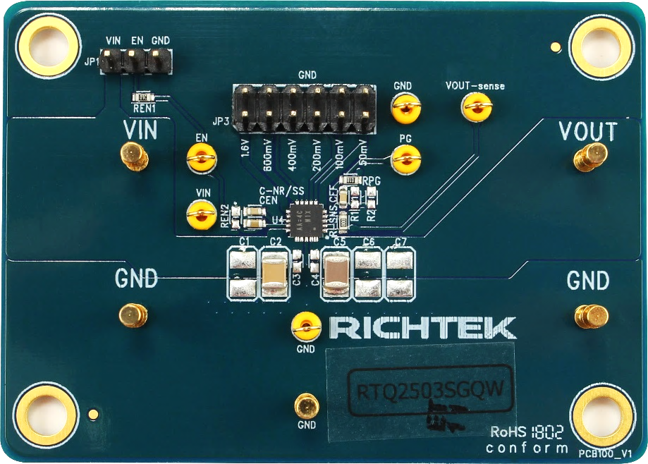
Carefully inspect all the components used in the EVB according to the following Bill of Materials table, and then make sure all the components are undamaged and correctly installed. If there is any missing or damaged component, which may occur during transportation, please contact our distributors or e-mail us at evb_service@richtek.com.
Test Points
The EVB is provided with the test points and pin names listed in the table below.
|
Test point/
Pin name
|
Signal
|
Comment (expected waveforms or voltage levels on test points)
|
|
VOUT
|
LDO output
|
LDO output terminal. A 22μF or greater of capacitance is at VOUT pin is required for stability.
|
|
VIN
|
LDO input source
|
LDO input terminal. Supply source available is (VOUT + 0.3V) ≤ VIN ≤ 6.5V.
|
|
EN (Test pin)
|
Enable test point
|
Enable control input. Connecting this pin to logic high enables the regulator or driving this pin low puts it into shutdown mode. Enabling the device after VIN are present is preferred.
|
|
GND
|
Ground
|
Ground. The exposed pad must be soldered to a large PCB and connected to GND for maximum the power dissipation.
|
|
PG (Test pin)
|
Power good indicator output
|
An open-drain output and active high when the output voltage reaches 88% of the target. The pin is pulled to ground when the output voltage is lower than its specified threshold, EN shutdown, OCP and OTP.
|
|
50mV, 100mV, 200mV, 400mV, 800mV, 1.6V
|
Output voltage setting pins
|
Connect these pins to ground or leave floating. Connecting these pins to ground increases the output voltage by the valueof the pin name; multiple pins can be simultaneously connected to GND to select the desired output voltage. Leave these pins floating (open) if the VOUT voltage is set by external resistor.
|
|
VOUT-sense
(Test pin)
|
Output voltage test point
|
LDO output voltage level monitoring point.
|
|
VIN (Test pin)
|
Input voltage test point
|
LDO input supply voltage monitoring point.
|
Output Voltage Setting
The output voltage of the RTQ2503S can be set by external resistors or by output voltage setting pins (50mV, 100mV, 200mV, 400mV, 800mV and 1.6V) to achieve different output target.
1. Setting output target by pins (50mV, 100mV, 200mV, 400mV, 800mV and 1.6V) :
The RTQ2503S also can short the pins pins (50mV, 100mV, 200mV, 400mV, 800mV and 1.6V) to ground and program the regulated output voltage level without external resistors after SNS pin is connected with VOUT pin .The pins pins (50mV, 100mV, 200mV, 400mV, 800mV and 1.6V) is connected with internal resistor pairs, each pin is either connected to ground (active) or left open (floating).
The voltage programming is set as the sum of the internal reference voltage (VREF = 0.8V) plus the accumulated sumof the respective voltages assigned to each active pin as illustrated in Figure 1.
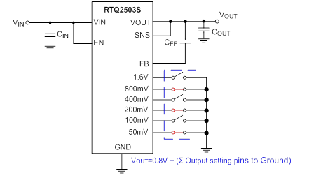
Figure 1. Output Setting without External Resistors
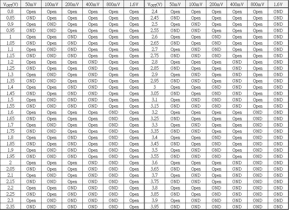
Table 1. summarizes these voltage values associated witheach active pin setting for reference. By leaving all programpins open, or floating, the output is thereby programmedto the minimum possible output voltage equal to VREF (0.8V). The maximum output target can be supported up to 3.95V after all pins pins (50mV, 100mV, 200mV, 400mV, 800mV and 1.6V) are shorted with groundat the same time.
Table 1. VOUT Select Pin Settings for Different Target
2. Using external resistors
The output voltage is determined by the values of R1, R2 and keeps SNS pin be floating as Figure 2. The values of R1and R2 can be calculated with any voltage value via use the formula by below equation and the suggested R1, R2 resistance is (R1 + R2) < 50kΩ :
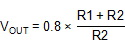
The suggested R1, R2 resistance is (R1 + R2) ≤ 50kΩ, the VOUT target range should be lower than (VIN - 0.3V) for good load transient response and output regulation ability.
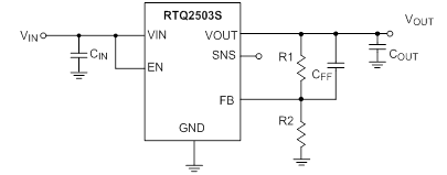
Figure 2. Output Voltage Set by External Resistors
Power-up & Measurement Procedure
1. Set the desired VOUT target value by JP6 that pull low the pins (50mV, 100mV, 200mV, 400mV, 800mV and 1.6V) with specific combination (reference the Table 1).
2. Connect input power (1.1V ≤ VOUT + 0.3V ≤ VIN ≤ 6.5V) and input ground to VIN and GND test pins respectively.
3. Connect positive end and negative terminals of load to VOUT and GND test pins respectively.
4. There is a 3-pin header “EN” for enable control. To use a jumper at “VIN” option to tie EN test pin to input power VIN for enabling the device. Inversely, to use a jumper at “GND” option to tie EN test pin and ground GND for disabling the device.
5. Verify the output voltage level between VOUT and GND.
6. Connect an external load up to 3A to the VOUT and GND terminals and verify the output voltage and current.
Schematic, Bill of Materials & Board Layout
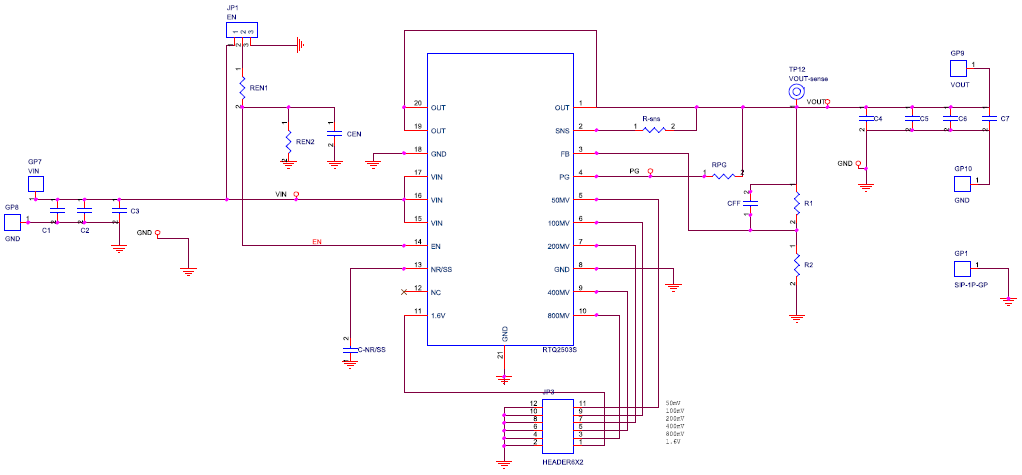
EVB Schematic Diagram
Bill of Materials
|
Reference
|
Qty
|
Part Number
|
Description
|
Package
|
Manufacturer
|
|
U4
|
1
|
RTQ2503SGQW
|
Linear Regulator
|
WQFN-20L 3.5x3.5
|
RICHTEK
|
|
CFF, C-NR/SS
|
2
|
0603B103K500CT
|
10nF/50V/X7R
|
C-0603
|
WALSIN
|
|
CEN
|
1
|
C1608X7R1H104K080AA
|
100nF/50V/X7R
|
C-0603
|
TDK
|
|
C2
|
1
|
GRM32ER61C476KE15L
|
47µF/16V/X5R
|
C-1210
|
Murata
|
|
C5
|
1
|
GRM32ER61C226KE20L
|
22µF/16V/X5R
|
C-1210
|
Murata
|
|
R-SNS
|
1
|
WR06X000PTL
|
0
|
R-0603
|
WALSIN
|
|
REN1
|
1
|
WR06X1002FTL
|
10k
|
R-0603
|
WALSIN
|
|
RPG
|
1
|
WR06X1003FTL
|
100k
|
R-0603
|
WALSIN
|
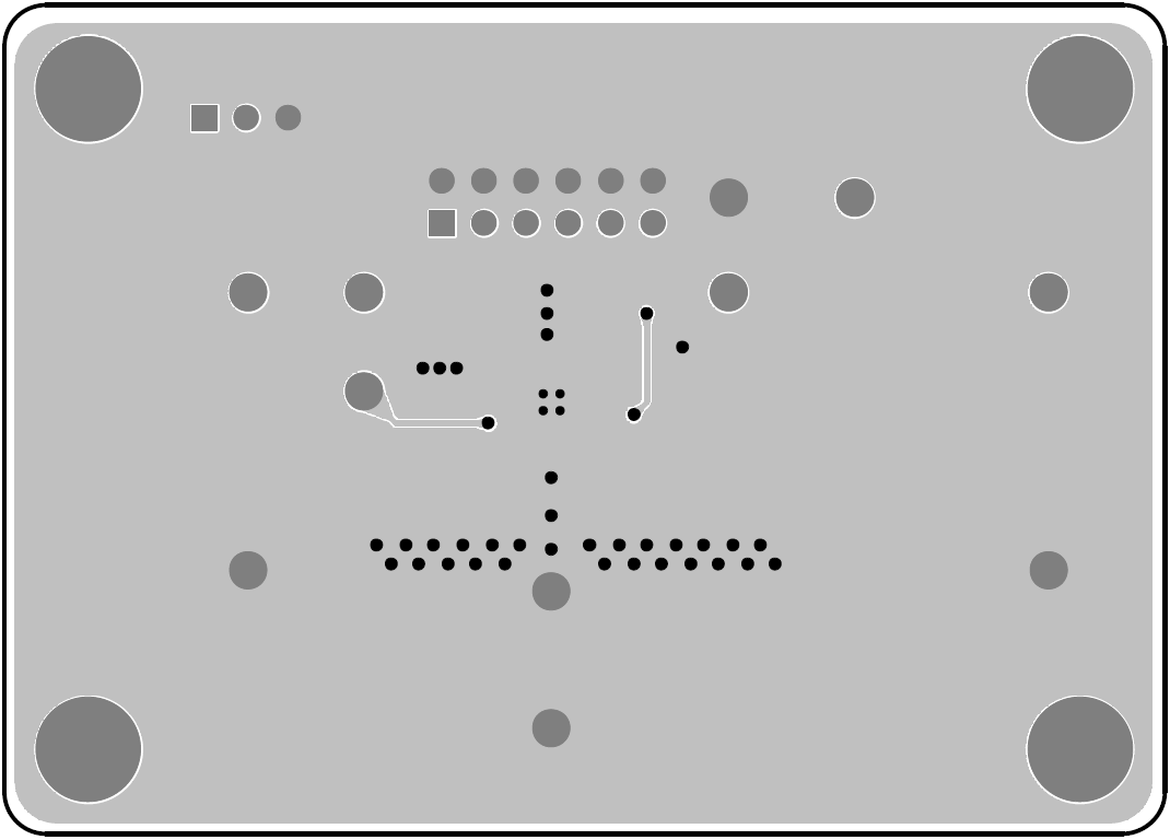
PCB Layout
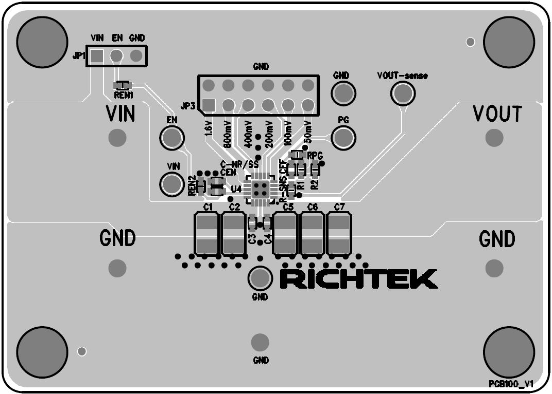
Top View (1st layer)

PCB Layout—Inner Side (2nd Layer)
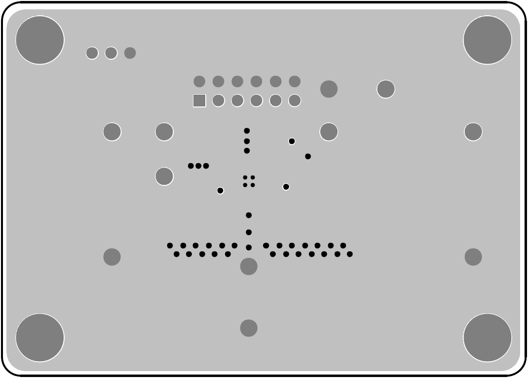
PCB Layout—Inner Side (3rd Layer)
Bottom View (4th Layer)